找回密码
 加入我们
搜索
      
查看: 16124|回复: 48

[CPU] igor's lab初步分析7800X3D烧U事件:烧毁的均为CPU供电针脚

[复制链接]
发表于 2023-4-24 22:49 | 显示全部楼层 |阅读模式
链接:https://www.igorslab.de/en/pin-a ... -core-power-supply/

原文:
The process with the destroyed Ryzen 7000X3D CPUs has of course already interested me and I didn’t want to just cover a news and that was it. So I took the damage picture from Reddit and put the back of the CPU in the right position first. We can see the destroyed Ryzen 7 and the dent along with the scorched copper pads in the picture. The picture of the scorched base didn’t help me at this point, since there was extensive damage there and you couldn’t make sense of anything at the end. For better understanding, I mirrored the front side and superimposed it semi-transparently using superposition. We see that the damage occurred just below the die.
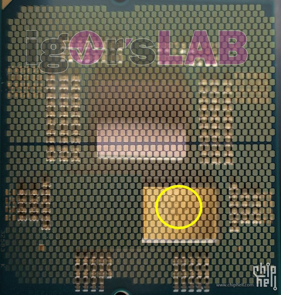

Damage-Small-1.jpg

Using another superposition, I then searched for the most affected pads. For this, I got the current pin assignment, whereby the documents from AMD can be quite confusing when comparing the individual revisions. Only the current revision was somewhat meaningful, because in some older versions not even the number of rows or pins was correct. But something like that can be solved. You also have to consider that the pins of the LGA are arranged 90° and possible burn marks on the pads can easily be on the side or outside of the copper, because the spring contacts have bent or shifted during the melting of the socket.

The pin diagram I assembled (AMD only supplies 4 individual quadrants here, which are unfortunately not even scaled to the same size) now shows the location of the damage once again. However, you have to take into account that the contacts in the socket are of course spatially offset from line, while the scheme is checkerboarded. If you consider the offset and possible displacements of the contacts, then the area marked purple by me in the picture below crystallizes. All affected contacts supply the CPU with the VDDCR (CPU Core Power Supply).

This raises the question why just the outer pins of the supply block were damaged in such a way. Whether the damage was caused in the socket or whether there was a short circuit in the CPU first is highly speculative and can hardly be answered plausibly by an outsider. Defective spring contacts or a bad assembly can actually be ruled out, since the error occurs too locally and also always shows the same damage pattern. Since motherboards from Asus and Gigabyte are also said to be affected, a faulty batch of sockets can almost be ruled out, so one should probably not conclude a serial defect. Personally, I would rather be interested in what the defective CPU looks like inside and if there are visible traces on the opposite side and on the die. And now, as always, there may be lively discussions.


简单总结:

igor lab对着AM5的针脚定义,发现被烧毁的78X3D背面的针脚均为VDDCR,即为CPU Core Power Supply针脚,用于CPU核心供电

igor lab认为插座和CPU的接触不良或用户安装CPU出问题不会是导致烧毁的原因,因为烧毁的CPU针脚均为同一位置

igor lab认为部分批次的插座出现接触不良的问题这一可能性也被排除,因为华硕和屏蔽牌的主板均受此影响

 楼主| 发表于 2023-4-24 22:54 | 显示全部楼层
AMD-RYZEN-7000X3D-PINMAP-IGOR.jpg
发表于 2023-4-24 22:55 | 显示全部楼层
Whether the damage was caused in the socket or whether there was a short circuit in the CPU first is highly speculative and can hardly be answered plausibly by an outsider.

实际上什么也没认定
发表于 2023-4-24 22:56 | 显示全部楼层
国外应该不会被打吧
 楼主| 发表于 2023-4-24 22:56 | 显示全部楼层
zerozerone 发表于 2023-4-24 22:55
Whether the damage was caused in the socket or whether there was a short circuit in the CPU first is ...

他手上没烧坏的U,只能推测了

现在只能等GN来个详细的分析了
发表于 2023-4-24 23:03 | 显示全部楼层
本帖最后由 zerozerone 于 2023-4-24 23:05 编辑

“ For this, I got the current pin assignment, whereby the documents from AMD can be quite confusing when comparing the individual revisions. Only the current revision was somewhat meaningful, because in some older versions not even the number of rows or pins was correct. ”

这段的意思盲猜:手头的AMD针脚的定义修订文件不保准,这个老版文件或许是非X3D的。推测了个寂寞。。。。

没这图,个人也能推测,然仅限于心里,发出来担心误导人。
发表于 2023-4-24 23:03 | 显示全部楼层
没啥好分析的,AMD SOP问题,上下游没沟通好,做过项目的都知道。如果写个PPT就是
root cause: 主板电压过高,击穿3D cache
interim solution: 让板厂把可调电压的BIOS和软件全部下架,
permanent solution: 发布类似x3D新SKU,需要强制更新agesa点亮,新agesa严格限制ccd电压,以免出现问题
我都给AMD的项目经理写好了,照抄就行了

至于为什么主板电压过高,那是因为CCD可以耐压,3D vcache不耐压。5800 x3d第一个能点亮的agesa只能跑3.3G,必须更新agesa才能正常工作。5800x3d发布那么久了,就这个电压致死的问题直到2023年3月31日igor labs才用msi的软件在windows下调出来,距今不到一个月。
至于am5主板电压给了高是因为按照之前发布zen4来优化的,如果说asus烧了多那也只能说明他优化工作做了多,验证做了多才有信心给了高。我是Lisa Su一封邮件发给zen4 msdt的项目总监,CC给工程部老大和CTO,明年年终奖扣多少你们心里清楚。
打人这次就替AMD背好锅就行了,反正消费者不懂项目流程,在坐的Partner们担待点。我Lisa Su保证zen5就算不改针脚,也不能用于6系主板,君不见zen3之于x370呼?让你们7系主板大卖。
 楼主| 发表于 2023-4-24 23:07 | 显示全部楼层
zerozerone 发表于 2023-4-24 23:03
“ For this, I got the current pin assignment, whereby the documents from AMD can be quite confusing ...

你这个就理解错了,他说的是AMD的老版针脚文件是有歧义让人困惑的,甚至针脚数都是错误的

他现在拿来用来推理的针脚文件是正确的
 楼主| 发表于 2023-4-24 23:09 | 显示全部楼层
zerozerone 发表于 2023-4-24 23:03
“ For this, I got the current pin assignment, whereby the documents from AMD can be quite confusing ...

7000和7000X3D都是一样的针脚定义,这么会有不同的针脚定义呢?你这就推测错了
发表于 2023-4-24 23:11 | 显示全部楼层
本帖最后由 pdvc 于 2023-4-24 23:12 编辑
T.JOHN 发表于 2023-4-24 23:03
没啥好分析的,AMD SOP问题,上下游没沟通好,做过项目的都知道。如果写个PPT就是
root cause: 主板电压过 ...


这一刻苏妈附身:华硕,你敢偷电压!背锅去吧!

华硕:为发烧而生
发表于 2023-4-24 23:11 | 显示全部楼层
上次4090烧供电Igor's Lab就给了一个自己的推测,但是自己没办法复现
后来GN不仅反驳了他们的推测,还提出了新推测并且复现了
不知道这次会不会一样
 楼主| 发表于 2023-4-24 23:12 | 显示全部楼层
Icarus_Radio 发表于 2023-4-24 23:11
上次4090烧供电Igor's Lab就给了一个自己的推测,但是自己没办法复现
后来GN不仅反驳了他们的推测, ...

GN舍得花钱从玩家手里买全套问题产品,给出的结论肯定是比igor这样隔空推测靠谱得多的
发表于 2023-4-24 23:13 | 显示全部楼层
本帖最后由 zerozerone 于 2023-4-24 23:29 编辑
T.JOHN 发表于 2023-4-24 23:03
没啥好分析的,AMD SOP问题,上下游没沟通好,做过项目的都知道。如果写个PPT就是
root cause: 主板电压过 ...


what?“am5主板电压给了高是因为按照之前发布zen4来优化的”

俺又猜中了???。。。。说得跟真的一样 哈哈

MSDT就不能多上点心。。。。。韭菜命苦
 楼主| 发表于 2023-4-24 23:14 | 显示全部楼层
zerozerone 发表于 2023-4-24 23:13
what?“am5主板电压给了高是因为按照之前发布zen4来优化的”

俺又猜中了。。。。 ...

那个是他推测的,目前还没有实锤,但不排除最后事实就是这样
发表于 2023-4-24 23:18 | 显示全部楼层
BFG9K 发表于 2023-4-24 23:14
那个是他推测的,目前还没有实锤,但不排除最后事实就是这样

都是猜,盲猜,盲人瞎马式的瞎猜。。。。
发表于 2023-4-24 23:18 | 显示全部楼层
pdvc 发表于 2023-4-24 23:11
这一刻苏妈附身:华硕,你敢偷电压!背锅去吧!

华硕:为发烧而生  ...


打人出货量大,其他板厂reddit上也有烧的,比如华擎,MSI事后还补BIOS限制电压,这是个共性问题,本质是x3d这个sku标准化生产的时候功课没做足,这还是zen4 x3D sku还是推迟发布的情况下发生的,项目组难辞其咎。
amd明明知道x3d vcache不耐压,5800x3d限了死,跑zen4上又给放开,这纯属它自己作死。板厂在zen4 x3d发布前已经释放的BIOS能好好地跑zen4,它一个新sku不更新agesa还能正常工作,被烧了如果指责板厂纯属拿前朝的剑斩本朝地官。
 楼主| 发表于 2023-4-24 23:20 | 显示全部楼层
T.JOHN 发表于 2023-4-24 23:18
打人出货量大,其他板厂reddit上也有烧的,比如华擎,MSI事后还补BIOS限制电压,这是个共性问题,本质是x ...

reddit上烧X3D的暂时只有华硕的案例,烧非X3D的倒是有其他品牌的板子
发表于 2023-4-24 23:21 | 显示全部楼层
本帖最后由 zerozerone 于 2023-4-24 23:25 编辑
T.JOHN 发表于 2023-4-24 23:18
打人出货量大,其他板厂reddit上也有烧的,比如华擎,MSI事后还补BIOS限制电压,这是个共性问题,本质是x ...


还是猜的呗。。。哈哈

其他厂推出限压新版固件,貌似他们有时间测试复现,找到问题实质?
还是临时措施,有枣没枣搂一杆再说?

so不能以板厂端的动作推演问题实质。
发表于 2023-4-24 23:27 | 显示全部楼层
T.JOHN 发表于 2023-4-24 23:18
打人出货量大,其他板厂reddit上也有烧的,比如华擎,MSI事后还补BIOS限制电压,这是个共性问题,本质是x ...

说到底就是3D不耐压 必须要限制一下  但是不是3D又需要开放电压才能释放性能   一个主板出场的时候刷哪个bios? 太难了  
发表于 2023-4-24 23:31 | 显示全部楼层
BFG9K 发表于 2023-4-24 23:20
reddit上烧X3D的暂时只有华硕的案例,烧非X3D的倒是有其他品牌的板子

虽然这个用户没有上烧针脚地图,但他打开华擎调试软件把7950x3d干挂了是真的,而且它还有7950x,同样跑过华擎调试软件没问题

https://www.reddit.com/r/Amd/comments/12ubu7h/comment/jhfufu2/
发表于 2023-4-24 23:33 | 显示全部楼层
Icarus_Radio 发表于 2023-4-24 23:11
上次4090烧供电Igor's Lab就给了一个自己的推测,但是自己没办法复现
后来GN不仅反驳了他们的推测, ...

你完全说反了
老黄早就按照igor的建议把3 dimple改为4 spring
intel也认证了写进atx3.0了

插不好一直都是第一假说 跟本不是gn的独有见解
gn只是在影片復现插不好的后果
gn自己的假说是接头有异物 他倒没有復现 老黄也没理gn

简单来说
gn一直不认为4 spring比3 dimple好而igor认为4 spring更好
最终结果就是老黄和intel都说4 spring比较好
发表于 2023-4-24 23:34 | 显示全部楼层
jxljk 发表于 2023-4-24 23:27
说到底就是3D不耐压 必须要限制一下  但是不是3D又需要开放电压才能释放性能   一个主板出场的时候刷哪个 ...

AMD可以用agesa锁的,给x3d锁电压,给其他型号解锁。类似于12/13th nonk的fivr让板厂连sa电压都调不了,agesa是个远比intel fivr功能强大得多的黑盒
 楼主| 发表于 2023-4-24 23:34 | 显示全部楼层
T.JOHN 发表于 2023-4-24 23:31
虽然这个用户没有上烧针脚地图,但他打开华擎调试软件把7950x3d干挂了是真的,而且它还有7950x,同样跑过 ...
t's not just ASUS.


I had a a 2 day old 7950X3D die on my x670 ASROCK Steel Legend, no OC Normal Usage, only bumped RAM to 6000mhz which is what the RAM is rated for.

I opened System Tune App from ASROCK and poof DEAD, No Overclock as I said, basically stock other than RAM.

I can't rule out it was just a bad defective CPU from the start that was maybe just sensitive to normal usage, voltage or temps, running a replacement 7950X3D for week but I am too scared to open that app again. The only thing I can say is that I tested the same Asrock System Tune Application on a regular 7950X and it did't kill that one. lol


看到了
发表于 2023-4-24 23:37 | 显示全部楼层
T.JOHN 发表于 2023-4-24 23:34
AMD可以用agesa锁的,给x3d锁电压,给其他型号解锁。类似于12/13th nonk的fivr让板厂连sa电压都调不了,a ...


你说的这个锁是指在物理上限制CPU吗   是指生产的时候限制? 如果是生产的时候限制  那这些没有物理限制的U   现在只能靠厂商的BIOS更新限制了吧

 楼主| 发表于 2023-4-24 23:39 | 显示全部楼层
jxljk 发表于 2023-4-24 23:37
你说的这个锁是指在物理上限制CPU吗   是指生产的时候限制? 如果是生产的时候限制  那这些没有物理限制 ...

他说的这个意思还是通过agesa来限制CPU电压,因为给多少电压是AGESA+BIOS决定的,不是CPU自己决定的
发表于 2023-4-24 23:41 | 显示全部楼层
jxljk 发表于 2023-4-24 23:37
你说的这个锁是指在物理上限制CPU吗   是指生产的时候限制? 如果是生产的时候限制  那这些没有物理限制 ...

非物理限制,agesa虽然是通过BIOS更新,但是通过AMD释放给板厂的,板厂无权修改。就好比最初的B450可以跑pcie4.0,但是之后amd通过agesa把pcie4.0给直接禁止了。
发表于 2023-4-24 23:41 | 显示全部楼层
BFG9K 发表于 2023-4-24 23:39
他说的这个意思还是通过agesa来限制CPU电压,因为给多少电压是AGESA+BIOS决定的,不是CPU自己决定的 ...

我明白了  通过这个agesa  可以让主板识别U是3D还是非3D再给电压是吧
 楼主| 发表于 2023-4-24 23:42 | 显示全部楼层
jxljk 发表于 2023-4-24 23:41
我明白了  通过这个agesa  可以让主板识别U是3D还是非3D再给电压是吧

是的,实际上MSI和ASUS最新的BIOS已经这样操作了
发表于 2023-4-24 23:42 | 显示全部楼层

动内存频率,联动的东西就多了 嘿嘿

另外初版固件的环境,APP怼参,绝对的勇士。
发表于 2023-4-24 23:44 | 显示全部楼层
T.JOHN 发表于 2023-4-24 23:03
没啥好分析的,AMD SOP问题,上下游没沟通好,做过项目的都知道。如果写个PPT就是
root cause: 主板电压过 ...

这PPT一看就是懂行的,AMD 这边又多一条lesson learn.
您需要登录后才可以回帖 登录 | 加入我们

本版积分规则

Archiver|手机版|小黑屋|Chiphell ( 沪ICP备12027953号-5 )沪公网备310112100042806 上海市互联网违法与不良信息举报中心

GMT+8, 2025-4-26 14:45 , Processed in 0.014571 second(s), 7 queries , Gzip On, Redis On.

Powered by Discuz! X3.5 Licensed

© 2007-2024 Chiphell.com All rights reserved.

快速回复 返回顶部 返回列表